Badge Design - step 3 (Or, hi-tech in Kunnamkulam)
Badge Design - step 3 (Or, hi-tech in Kunnamkulam)
2006-11-09T18:41:00
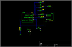
Finally, I have made some sense out of gschem and pcb, the gEDA tools. Schematic capture is easy; what is difficult is using PCB. Here is the schematic of the badge:
 A major problem with pcb is lack of footprints for some of the parts used in the circuit - the microswitch and the button cell holder. I was able to solve this by modifying some footprints available from gedasymbols.org. Gschem too doesn't come loaded with symbols - you have to manage by tweaking whatever is available (or making your own - in the true spirit of free software).
I took the design files with me to a pcb design centre in Kunnamkulam - it was my first visit to the place. It was well worth the time because the owner of the design house was a very knowledgeable and enthusiastic self taught electronics guy. I was surprised to know that there is a lot of industrial demand even in our low-tech God's own country for microcontrollers from all the major manufacturers - Atmel and Microchip being the favourites! I got two suggestions - one, to dump the auto-router and use hand-routing and two - to change the dimension of the padding around the pins to accommodate for the sloppy soldering which I will be doing ... one more sleepless night changing footprint files ...
Is autorouting in two-dimensions some kind of intractable problem? It was interesting to observe pcb perform the routing in a flash when given two layers and slowing down considerably when given just one layer.
A major problem with pcb is lack of footprints for some of the parts used in the circuit - the microswitch and the button cell holder. I was able to solve this by modifying some footprints available from gedasymbols.org. Gschem too doesn't come loaded with symbols - you have to manage by tweaking whatever is available (or making your own - in the true spirit of free software).
I took the design files with me to a pcb design centre in Kunnamkulam - it was my first visit to the place. It was well worth the time because the owner of the design house was a very knowledgeable and enthusiastic self taught electronics guy. I was surprised to know that there is a lot of industrial demand even in our low-tech God's own country for microcontrollers from all the major manufacturers - Atmel and Microchip being the favourites! I got two suggestions - one, to dump the auto-router and use hand-routing and two - to change the dimension of the padding around the pins to accommodate for the sloppy soldering which I will be doing ... one more sleepless night changing footprint files ...
Is autorouting in two-dimensions some kind of intractable problem? It was interesting to observe pcb perform the routing in a flash when given two layers and slowing down considerably when given just one layer.
Tom
Mon Dec 8 01:51:59 2008
Sir, I am also residing at thrisssur. I have so few electronics friends that I can't develope in this field. No I wan't know that from where I get a less costly PCB manufacturer? In Hitech Kunnamkulam or any other place in thrissur?